
Product Specification
Product Description
Application Field
Why Choose Us
Product Description
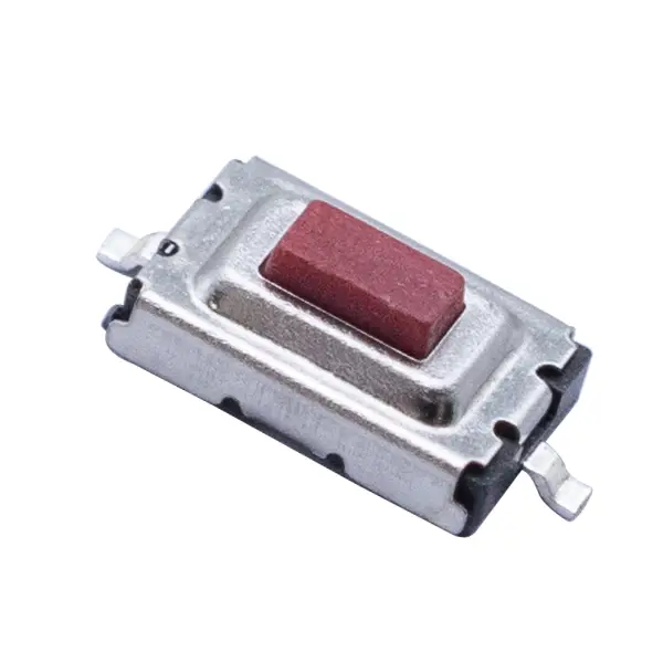
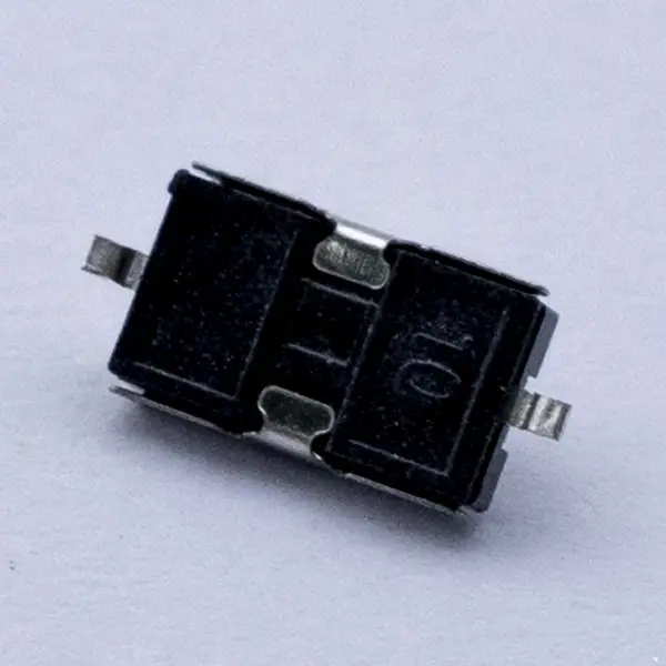
This ultra-compact, surface‑mount tactile switch delivers a consistent, precise click for modern keyboard modules and keypads. Its low profile fits beneath scissor or hinge mechanisms, while tight force control and minimal wobble ensure uniform feel across large key arrays. Optimized contact design supports high‑speed matrix scanning with low bounce for accurate keystroke detection.
Key Features
- Compact SMD package: 3.0 × 2.0 × 1.5 mm (L × W × H)
- SPST‑NO, momentary, top‑actuated
- Rated 12 VDC / 50 mA (suitable down to low‑level signal currents)
- Short, crisp travel for fast actuation; tactile bump for clear feedback
- Actuation force options: 130 gf (Light), 180 gf (Standard), 260 gf (Firm)
- Tight force consistency for uniform keyboard feel
- Low bounce for clean matrix scanning (typical ≤5 ms)
- Long life: 300,000 actuations (room conditions, standard force)
- Minimal stem tilt and wobble for stable keycap engagement
- Operating temperature: −40 to +85°C
- RoHS and REACH compliant; halogen‑free
- Tape‑and‑reel packaging for automated placement
Electrical and Mechanical Specifications
- Contact rating: 12 VDC, 50 mA max
- Contact resistance: ≤100 mΩ initial (≤200 mΩ after life test)
- Insulation resistance: ≥100 MΩ at 100 VDC
- Dielectric withstand: 250 VAC for 1 minute
- Pre‑travel (to tactile bump): approx. 0.15 mm (typical)
- Total mechanical travel: approx. 0.25 mm (typical)
- Actuation forces: 130 / 180 / 260 gf (±20% tolerance)
- Bounce time: ≤5 ms typical
- Operating life: 300k cycles (standard force, 2 Hz), application‑dependent
Materials and Construction
- Housing: high‑temperature LCP, black
- Plunger: PA46/PPA engineering resin
- Contacts: silver‑plated copper alloy (gold‑plated contact option on request for low‑level/low‑corrosion environments)
- Terminals: copper alloy with Ni underplate and matte Sn finish (lead‑free)
Recommended Keyboard Integration
- Matrix scanning: 0.5–2 kHz poll rate recommended; implement 5–10 ms firmware debounce
- Pull‑ups/pull‑downs: 1–10 kΩ typical; ensure stable logic thresholds for low‑current operation
- Anti‑ghosting: use per‑key diodes in large matrices or appropriate firmware to avoid ghost keys
- Keycap interface: center the plunger load; target misalignment within ±0.3 mm to minimize side load
- Over‑travel design: allow 0.1–0.3 mm additional keycap travel beyond electrical actuation using a compliant mechanism; avoid hard bottoming on the switch
- ESD: add board‑level protection (e.g., TVS diodes) where the key surface is user‑exposed
- Recommended plunger contact area: 1.4–1.8 mm diameter, flat or slightly domed
Soldering and Assembly Guidelines
- Reflow (Pb‑free): peak 245°C; 60–90 s above 217°C; ≤2 reflow cycles
- Hand rework: 350°C max tip, ≤3 s per pad; do not press the actuator during soldering
- No wave soldering; not suitable for immersion or ultrasonic cleaning
- Place and reflow on flat PCB; keep external forces off the actuator during process
Reliability and Environmental Qualification
- Operating life: 300k cycles at 2 Hz (standard test)
- Thermal shock: −40°C to +85°C, multiple cycles; no functional damage
- Damp heat: 40°C, 90–95% RH, 96 h; maintains insulation properties
- Vibration: 10–55 Hz, 1.5 mm amplitude, 2 h per axis; no contact chatter beyond spec
- Mechanical shock: 100 g, 6 ms, multiple axes; no structural damage
- ESD robustness (device‑level qualification): up to ±6 kV contact, ±8 kV air per IEC 61000‑4‑2 in our lab tests; board‑level protection still recommended
- Post‑test limits: contact resistance ≤200 mΩ; no sticking or intermittent failures observed in qualification
Footprint and Layout
- Recommended land pattern: two SMT pads approx. 0.9 × 1.0 mm with ~1.8–1.9 mm pad‑to‑pad spacing (center‑to‑center)
- Keep‑out: no copper under the actuator area (~1.5 × 1.5 mm) to avoid interference
- Maintain flatness and coplanarity; follow IPC‑7351 guidelines for pad fillet
Packaging
- Embossed tape: 8 mm width, 4 mm pitch
- Reel quantity: 3,000 pcs/reel (typical)
- Orientation marked on carrier; no polarity
Compliance and Quality
- RoHS and REACH compliant; halogen‑free materials
- Manufactured in ISO 9001‑certified facilities
- Lead‑free, matte‑tin finish compatible with Pb‑free reflow
Ordering Information
- Base model: Precision SMD Tact Switch, 3 × 2 × 1.5 mm, SPST‑NO
- Force options: L = 130 gf, S = 180 gf, F = 260 gf
- Contact plating: S = Ag standard, G = Au option
- Example code: TS‑3020‑S‑180 (standard plating, 180 gf)
Note: Exact ordering codes and availability may vary; confirm with sales before purchase.
Use Cases
- Laptop‑style scissor keyboards and compact key modules
- Industrial control panels and membrane keyboard arrays
- POS terminals, medical instruments, and instrumentation keypads
- Custom macro pads, compact gaming key clusters