Designing PCB Footprints for Tact Switches: A Definitive Guide
To design a PCB footprint for tactile switches, you must prioritize mechanical stability alongside electrical connectivity. Essential steps include verifying manufacturer datasheets for exact pin pitch, extending solder pads by 0.2mm to 0.5mm at the "toe" to increase shear strength, and defining a courtyard that prevents component collision during actuation. Always validate the footprint against the physical component before mass production.
Why Is Accurate Footprint Design Critical for Switches?
Designing a footprint for a resistor is simple; designing one for a tactile switch is an engineering challenge. Unlike static components, switches are dynamic mechanical devices. They are subjected to repeated physical force (actuation) by the user.
If the footprint relies solely on standard IPC tolerances without accounting for actuation force, the switch may eventually shear off the pads.
According to internal durability testing conducted by HX Switch, over 40% of field failures in consumer electronics are due to pad lifting caused by insufficient solder fillet area, not internal component failure. Therefore, the footprint must be designed to act as a mechanical anchor.
What Are the Key Elements of a Tact Switch Footprint?
When creating your library part in software like Altium, KiCad, or Eagle, you must focus on three specific layers.
1. The Copper Pads (Land Pattern)
The pads must match the lead width but allow for a robust solder fillet.
- For SMD Switches: We recommend the "Fillet Extension Rule." Add an extra 0.3mm to 0.5mm to the length of the pad extending away from the switch body (the "toe"). This allows for a larger solder slope, significantly increasing mechanical holding force.
- For Through-Hole Switches: Ensure the annular ring is at least 0.3mm larger than the drill hole to prevent pad lifting during wave soldering or rework.
2. The Solder Mask
The solder mask opening should generally be 0.05mm to 0.1mm larger than the copper pad (1:1 scale is risky due to registration errors).
- Unique Insight: For high-density boards, HX Switch engineering recommends using "Solder Mask Defined" (SMD) pads for the ground terminals if they are used for shielding. This locks the copper to the FR4 substrate more securely.
3. The Courtyard (Keep-Out Zone)
The courtyard defines the physical space the switch occupies.
- Height Clearance: Remember that the actuator moves. Ensure no components hang over the switch.
- Actuation Buffer: Leave a 1mm buffer zone around the switch to accommodate the user’s finger or the device casing button.
Step-by-Step: How to Calculate Pad Dimensions
Follow this process to ensure your footprint is production-ready.
- Consult the Datasheet: Never guess. Locate the "Recommended Land Pattern" section of the datasheet.
- Apply IPC-7351B Guidelines (With a Twist): While IPC standards are excellent, they are generic. For switches, use the "Most Material Condition" (Density Level A) to ensure maximum solder volume.
- Adjust for Assembly Type:
- If you are reflow soldering, ensure thermal reliefs are balanced to prevent "tombstoning."
- For manual assembly tips, refer to our guide on how to solder SMD tact switches to understand how pad thermal mass affects the joint.
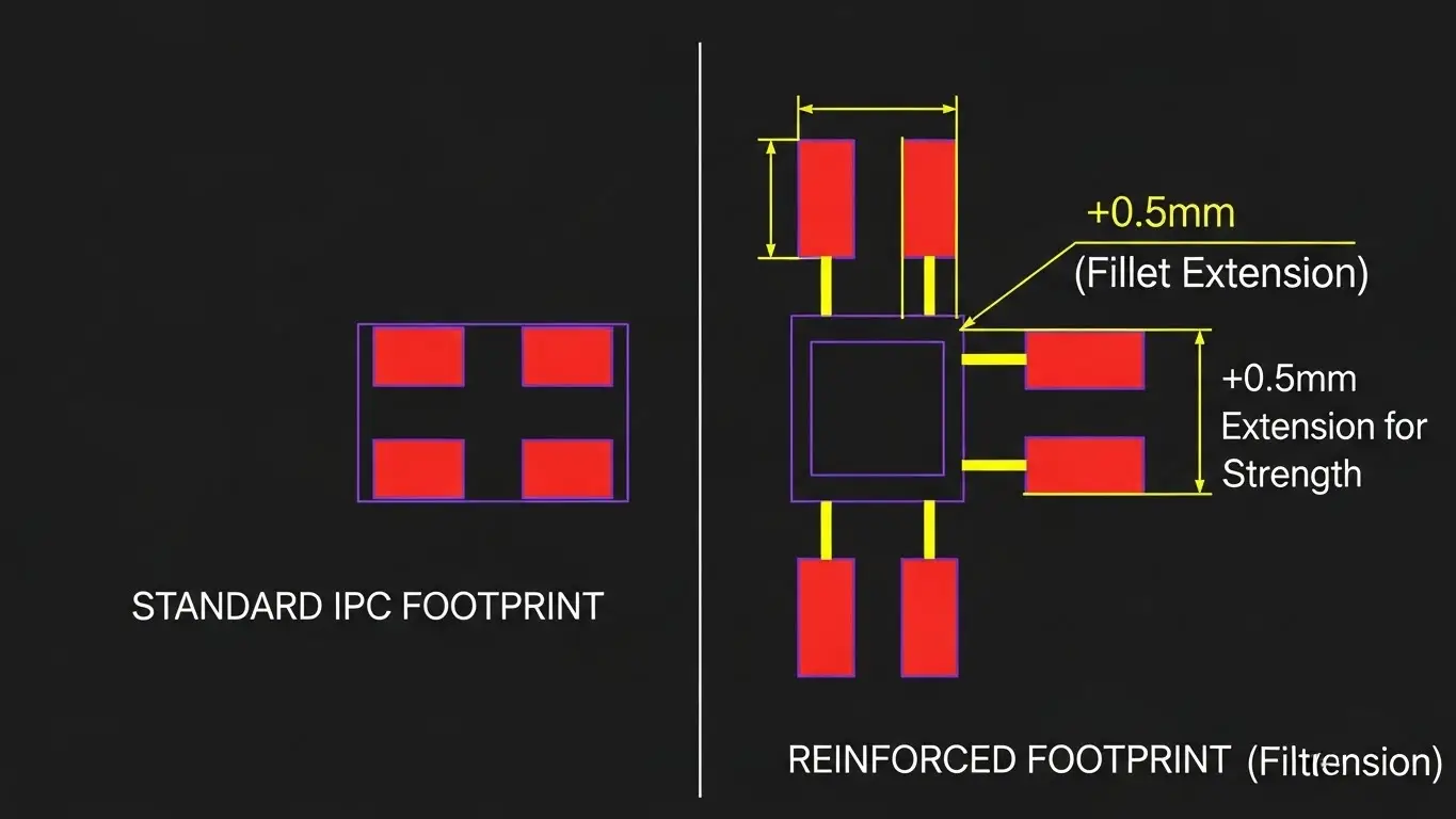
Comparison: Standard vs. Reinforced Footprints
| Feature | Standard IPC Footprint | HX Switch Reinforced Footprint |
| Pad Toe Length | Standard (approx. +0.1mm) | Extended (+0.3mm to +0.5mm) |
| Solder Mask | Non-Solder Mask Defined | Mask Defined (for anchors) |
| Application | Static parts (Resistors/ICs) | Dynamic parts (Switches/Connectors) |
| Shear Strength | Moderate | High (Resists thumb pressure) |
Common Mistakes to Avoid in Layout Design
Ignoring the "Boss" (Locating Pin)
Many tactile switches come with small plastic posts on the bottom called "bosses" or locating pins. These require non-plated holes in your footprint.
- The Error: Designers often forget these holes, causing the switch to sit tilted on the PCB.
- The Fix: Always verify if your specific part number includes bosses.
Incorrect Hole Sizes for Snap-In Pins
Some through-hole switches use "kinked" leads to snap into the board before soldering.
- If the hole is too loose, the switch falls out during assembly.
- If the hole is too tight, the leads deform.
- For guidance on drilling and mounting, see our industrial switch installation guide.
Forgetting Testing Points
Once the switch is soldered, you need to verify it works.
- Design Tip: Add small test points or vias connected to the switch nets. This allows you to check continuity without probing the delicate switch legs directly.
- Verification: Learn the proper testing protocols in our article on how to test a DIP switch with a multimeter.
Integrating Switches into Complex PCBs
When designing boards that mix different switch types, consistency in footprint orientation is key.
If your board includes both momentary tact switches and configuration switches, ensure the "ON" positions are oriented logically (e.g., all "Up" is "ON"). For configuration specifics, review how to configure DIP switch positions.
Furthermore, successful implementation goes beyond just the footprint. It involves understanding the physical installation process. Before finalizing your Gerber files, we strongly suggest reviewing how to install a tact switch on PCB to visualize the physical constraints of the assembly process.
Frequently Asked Questions (FAQ)
The most common pin pitch configurations for through-hole tact switches are 6.5mm x 4.5mm or 5.0mm x 5.0mm. However, for Surface Mount (SMD) variants, the pitch varies significantly by manufacturer. Always verify with the specific component datasheet.
For the signal pins, use thermal relief to make soldering easier. However, for the anchor/ground pins (if applicable), HX Switch recommends solid connections (direct connect) if your soldering process allows it. This provides better mechanical adhesion to the board, preventing the switch from ripping off during vigorous use.
The silkscreen (legend) should clearly outline the switch body so assemblers know the orientation. Crucially, ensure no silkscreen ink is placed over the solder pads. Ink on the pads acts as an insulator and will cause solder joint failure.
It is risky. Generic libraries often assume "Nominal" material conditions. Because tactile switches are mechanical interfaces, it is safer to create a custom footprint with extended pads to handle the mechanical stress of user actuation.