PCB Layout Tips for SMD DIP Switches
Designing a reliable PCB layout for SMD DIP switches requires more than just dragging a footprint from a library. Success relies on three engineering pillars: optimizing pad geometry to prevent solder bridging, implementing proper thermal relief to protect the housing, and ensuring robust mechanical anchoring.
Unlike passive resistors or capacitors, switches are active mechanical components. They must withstand the physical shear force of a user's finger or a screwdriver. If your land pattern (footprint) is too small, the switch may shear off the board during actuation; if the paste aperture is too large, the switch may float or "tombstone" during reflow. To ensure long-term reliability, engineers must follow IPC-7351 standards while adding 10-15% extra pad area for mechanical stability on the anchor points.
Why Is Pad Geometry Critical for SMD Switches?
Pad geometry dictates the mechanical strength of the solder joint, which is the only thing holding an SMD switch to the board.
When a user pushes a lever or slider, they generate lateral force. If the copper pads are undersized, the copper foil itself can delaminate from the FR4 material.
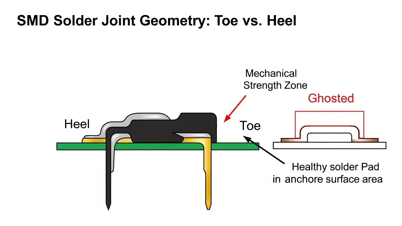
The "Toe and Heel" Rule
For Surface Mount Device (SMD) switches, the "heel" (inner part of the pad) handles the electrical connection, while the "toe" (outer part) handles the mechanical leverage.
- Extend the Toe: We recommend extending the pad length outward by 0.5mm beyond the manufacturer's minimum recommendation. This creates a larger solder fillet, acting as a structural buttress.
- Check the Actuation Force: High-force switches require larger pads. As we discussed in our guide on how tact switch actuation force works, a switch requiring 500gf needs significantly stronger anchoring than a 100gf switch to prevent pad lifting.
How Do I Handle Thermal Management During Reflow?
You must strictly adhere to the manufacturer’s reflow profile (usually <260°C peak) and use thermal relief on ground planes to prevent uneven heating.
Uneven heating causes two major issues for DIP switches:
- Housing Warp: The plastic body of a DIP switch (often PPS or Nylon) is heat-sensitive. Excessive heat can warp the casing, jamming the internal sliders.
- Tombstoning: If one pad is connected to a large ground plane without thermal relief, it heats up slower than the signal pad. The solder on the signal pad melts first, pulling the component upright and disconnecting it.
Pro Tip: If your switch needs to be washed after reflow to remove flux, ensure you have selected a sealed version. Check our article onhow IP67 waterproof rating works for tact switchesto understand the difference between process-sealed and standard switches.
What Are the Rules for Keep-Out Zones?
You need a clear area of at least 1mm to 2mm around the switch body to accommodate pick-and-place nozzles and allow for manual actuation tools.
Engineers often pack components too tightly. While a resistor doesn't need "finger room," a DIP switch does.
- Nozzle Clearance: Automated assembly machines use vacuum nozzles to place the switch. If tall capacitors are placed immediately next to the switch, the nozzle may collide with them.
- Actuation Access: Whether you are using momentary vs. latching tact switches or standard DIPs, the user needs space to access the actuator without shorting out nearby components with a screwdriver.
Common Layout Mistakes to Avoid
Even experienced designers make these errors when rushing a board layout.
1. Ignoring Solder Mask Dams
DIP switches often have a pitch (distance between pins) of 1.27mm (half-pitch) or 2.54mm. On half-pitch switches, the gap between pads is tiny. If you do not define a solder mask dam (a strip of green masking) between the pads, solder will flow between them, causing shorts.
2. Missing Pin 1 Indicators
DIP switches are polarized. Always put a clear silk screen dot or arrow indicating "ON" position or Pin 1. Do not rely on the component marking alone, as it may be obscured by flux residue or labels.
3. Placing Vias Under Pads
Never place an open via inside the mounting pad (Via-in-Pad) unless it is capped and filled. During reflow, the liquid solder will wick down into the hole (capillary action), leaving the joint "starved" of solder and weak.
Comparison: Half-Pitch vs. Full-Pitch Layouts
Choosing the right pitch affects your routing density and ease of assembly.
| Feature | Full-Pitch (2.54mm) | Half-Pitch (1.27mm) |
| Space Efficiency | Low (Takes up more PCB real estate) | High (Ideal for compact IoT devices) |
| Routing | Easy (Traces can run between pads) | Hard (Requires tight tolerances) |
| Solder Bridging Risk | Low | High (Requires high-quality stencil) |
| Hand Soldering | Easy | Very Difficult |
Ensuring Long-Term Reliability
The layout also impacts the longevity of the switch. If the board flexes, rigid SMD joints can crack.
- Board Flexure: Place switches near the mounting screws of the PCB, where the board is stiffest. Placing an SMD switch in the center of a large, unsupported PCB area can cause solder joints to crack when the user presses down.
- Maintenance: Consider the tact switch lifecycle ratings. If a switch is rated for only 2,000 cycles, it might need replacement. Design the footprint with slightly larger pads to make desoldering and hand-reworking easier for technicians later.
For a broader understanding of switch mechanics and how they influence PCB design, you can read our Micro Switch Deep Dive.
Frequently Asked Questions
A stainless steel stencil thickness of 0.12mm to 0.15mm is typically ideal. This ensures enough solder paste volume to create a strong mechanical fillet without causing bridging between fine-pitch pins.
Yes, but it is difficult, especially for half-pitch (1.27mm) types. It is best to use a "drag soldering" technique with plenty of flux and a fine-tip iron. However, reflow ovens provide much more consistent results.
Generally, no. The solder joint should be sufficient. However, for high-vibration environments (like automotive), you may add adhesive dots under the switch body before reflow to provide extra mechanical security.
Flux residue can gum up the contact mechanism. The best defense is a proper layout that prevents flux from flowing under the body, and using top-tape sealed switches that prevent liquids from entering the actuator area during washing.
This is usually caused by "Pad Cratering" or delamination. It happens when the actuation force is too high for the pad size. Increase the copper pad area or add "sewing vias" (stitched vias) to the ground plane to anchor the pad more firmly to the board substrate.
Key Takeaways
- Pad Size: Increase the "toe" of the pad by 10-15% to increase mechanical holding strength against actuation force.
- Clearance: Leave a 1-2mm keep-out zone around the switch for nozzles and fingers.
- Masking: Always ensure there is a solder mask dam between pins, especially on 1.27mm pitch switches, to prevent shorts.
- Location: Place switches near PCB mounting holes to reduce board flex stress during pressing.
Conclusion
A perfect PCB layout for SMD DIP switches balances electrical connectivity with mechanical durability. By respecting keep-out zones, optimizing solder fillets for shear strength, and managing reflow temperatures, you ensure your device remains reliable in the field.
If you are dealing with tight spaces or harsh environments, review your component selection carefully—sometimes a through-hole switch is structurally necessary, or a sealed IP67 switch is required for process safety.